Tuesday, November 22, 2011

IC Prog Settings for pic programmer


Discription :
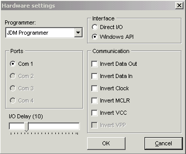
You need the following settings in IC Prog, (select JDM Programmer and Windows API)
IC Prog Programmer hardware menu settings
Note: If you have more ports you need to select correct com port.
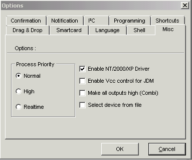
  • When using NT, 2000, XP you need Installing Driver
Download the Windows NT/2000/XP Driver. Put the NT/2000 driver file (icprog.sys) in the same directory as the ICProg.exe file. In ICProg, click on ‘Settings’ in the main window and open the‘Options’ window. Select the ‘Misc‘ tab. Click ‘Enable NT/2000/XP Driver‘. ICProg will then restart with the new driver and everything should be peachy.
IC Prog Installing Driver for NT, 2000, XP
  • When using Vista and Windows 7 you need to installing IC Prog 1.06.
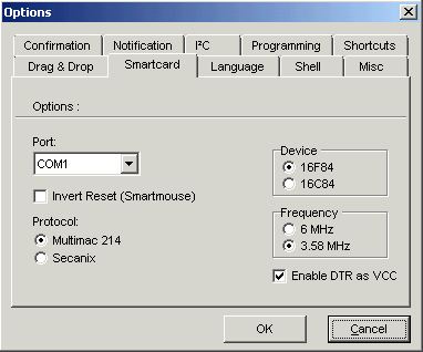
Configure Ic-prog Smartcard tab
In ICProg, click on ‘Settings’ in the main window and open the ‘Options’ window. Select the ‘Smartcard‘ tab.
Example: You need the following settings when using PIC16F84 or PIC18F84A
ic-prog smartcard setting for pic16f84
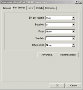
Configure the serial port in Computer
Go to the Device Manager (Start→SettingsControl PanelDevice Manager)
Ports (Com & LPT)Double click on communications port (Com 1 or 2 )  Port
configuration tab
com port configuration tab settings for ic prog
Verify the following values:
Bits per second: 9600
Data bits: 8
Parity: None
Stop bits: 1
Flow control: none
Test the Programmer
  • connect the programmer to computer
  • Start the IC Prog software
  • do a preliminary check of the serial interface by selecting Settings → Hardware Check from the menu.  The following dialog box will come up:
IC Prog Hardware Check enable clock
  • Turn on “Enable Clock” by selecting the check box. This will allow the power and LED to be turned On or Off. If this does not work check LED and PIC Programmer Circuit.
Programming the microcontroller using IC Prog,
  • Select the device (microcontroller) to be programmed. (Settings→ Device)
  • Open the code file (hex file) to be written in the PIC.
    Oscillator and Configuration bits are changed as indicated by the *.hex file. We can
    maintain these values, or change them later if we have problems during the
    programming proccess.
  • Programming the microcontroller,
    press Program All button or F5.
IC Prog Program All button
During the programming, some messages will be shown:
  • Device writing confirmation (if enabled)
  • Programming code progress bar
  • Programming data progress bar
  • Programming configuration
  • Verifying code (if enabled)
  • Verifying data (if enabled)
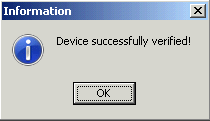
IC-Prog will show the following dialog box if the verification is successful.
ic prog successfully verified message
PIC Programming is done. Now you can use this PIC IC for your circuit.
If the verification fails, don’t worry, no permanent damage is done.  There are two common verification failures – data and code.  A data verification failure can be safely ignored and just means that the EEPROM was not fully zeroed.  The message displayed will say “Verify failed at data address XXXXh”.  Note the word “data” in front of “address”.
ic prog Verify failed at data address XXXXh
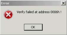
If the message says “Verify failed at address XXXXh”, note that the word “data” is not in front of “address”, then the code verify failed and there is some sort of problem.
IC Prog Verify failed at address XXXXh message
Errors solutions:
General
  • Erase the PIC before writing it
  • Close all other applications running on the PC
Hardware
  • Check the cable connections and the number of the serial port
  • Check the model of PIC that we are programming
  • Check the PIC position on the socket
  • Check that all the pins are correctly inserted on the socket
Software
  • Check the type of PIC.
  • Check Menu → Settings → Type of hardware.
  • Check the number of serial port selected.
  • Check that the file code (*.hex) is correct. It’s no good writing a *.txt file in the
    PIC.

Sunday, November 20, 2011

Capacitors

Discription :
A Capacitor is a passive two terminal component which sotres electric charge.This component consists of two conductors which are separated by a dielectric medium.The potential difference when applied across the conductors polarizes the dipole ions to store the charge in the dielectric medium.The circuit symbol of a capacitor is shown below :
The capacitance or the potential storage by the Capacitor is measured in farads which is symbolized as F .One Farad is the capacitance when one coulomb of electric charge is sotred in the conductor on the application of one volt potential difference.
The charge stored in a capacitor is given by

Q=CV
Where  Q= charge stored by the capacitor
            C= capacitance value of the capacitor
            V=Voltage applied across the capacitor
Note the other formula of current,     I=dQ/dt
dQ/dt=d(CV)/dt
Form the above statment,we can express the equation as
I=C9dV/dt)
As you turn on the power supply,the current begins to flow through the capacitor inducing the positive and negative potentials across its plates.The capacitor continues to charge until the capacitor voltage equalizes up to the supply voltage which is called as the charging phase of the capacitor.Once the capacitor is fully charged at the end of this phase,it gets open circuited for DC.It begins to discharge when the power of the capacitor is switched off.The charging and discharging of the capacitor is given by a time constant.

t=Rc the voltage across the capacitor is given by


Capacitors are widely used in a variety of applications of electronics circuits such as
store charges such as in a camera flash circuit
smoothing the output of power supply circuits
coupling of two stages of a circuit (coupling of an audio stage with a loud speaker)
filter networks (tone control of an audio system )
delay applications (as in 555 timer IC controlling the charging and discharging )
tuning radios to particular frequencies
phase alteration

The conductors offer a series resistance and if the capacitor is constructed using tubular structure then some inductance is also induced.The dielectric medium between the plates has an electric field strength limit and also passes a small amount of leakage current which results into a breakdown voltage .
The capacitor can be fixed or variable.They are categorized into  two groups,polarized or non-polarized.Electrolytic capacitors are polarized.Most of the low value capacitors are non-polarized.The symbol of capacitors from each group is shown below :

Construction and Types :
The capacitor consists of two conducting plates that are separated by an insulating medium know as the dielectric.The capacitance is dependent upon the surface area of the plates,the distance between the dielectric medium and the dielectric constant of the object.The greater the area of the plates,the closer they are together and greater the value of the dielectric constant the greater is the value of capacitance.High capacitance capacitors are now avialable in small size .This has been achieved employing a number of techniques like having several sets of plates,placing the plates very close to one another,having a thin layer of dielectric placed between them and developing special insulating dielectric materials.

The capacitance of a capacitor is also affected by the shape or structure of the capacitors.The capacitors are available in diffrent shapes like radial lead type which are rectangular or cubical or axial type which are tubular or cylindrical.
The variable type of capacitors can vary the capacitance by chanding the distance between the plates or the effective area of the capacitor.
The polarized type of capacitors should be connected as per thier polarity or else the capacitor can be damaged due to incorrect connection .
The low value capacitors are non-polarized and can be connected in any manner.They are not damaged by heat when soldering,except for the polystyrene type of capaciotr.They have high voltage ratings of at least 50V,usually 250V or so ,Many small value capacitors have thier value printed but without a multiplier,s you need to use experience to work out what the multiplier should be
For example :
0.1 means 0.1 uF=100nF
Sometimes the multiplier is used in place of the decimal point :
For example 4n7 means 4.7 nF


1. Variable Capacitors :

The various types of capacitors are given below :
  1. Fixed capacitors :Flim Capacitors like glass capacitor,mica capacitors,silver mica capacitor,ceramic capacitor,papaer capacitor,metalized paper capacitor,polyester capacitor,polystrene capacitor,metalized polyester capacitor,polcarbonate capacitor,polypropylene capacitors,teflon capacitors,porcelain capacitor,electrolyte capacitors like aluminum electrolyte,tantalum electolyte,aluminum-tantalum
  2. Variable Capacitors :
The variable type of capacitors can vary the capacitance by changing the distance between the plates or the effective area of the capacitor.
a.Air-gap capacitors :
These capacitors user air as the dielectric medium.The capacitance values iffered are high and can be used with high voltages.These are used for high frequency operation in communication systems.
b. Vacuum capacitors :
these capacitors have glass or cerramic encapsulation and vacuum as the dielectric.Their complex construction makes it very expensive .The oretically,it has less losses and are used in RF applications.


Capacitor color code :

A color code was used on polyester capacitors for many years.It is now obsolete,but of course there are many still around.The colors should be read like the resistor code.
  • The top three color nabds give the value in pF
  • The 4th band is for tolerance.
  • The 5th band is for the voltage rating.
For example :
brown,black,orange,means 10000pF=10nF=0.01uF
Note : There are no gaps between the color bands,so 2 identical bands actually appear as a wide band.
Wide red,yellow means 220nF=0.22uF


Monday, November 14, 2011

Diodes

Function :
Diodes allow electricity to flow in only one direction.The arrow of the circuit symbol shows the direction in which the current can flow.Diodes are the electrical version of a valve and early diodes were actually called valves.
Symbole :
Characteristic of Silicon Diode :

Forward Voltage Drop:
Electricity uses up a little energy pushing its way through the diode,rather like a person pushing through a door with a spring.This means that tere is a small voltage across a conducting diode,it is called the FORWARD VOLTAGE DROP and is about 0.7v for all normal diodes which are made from silicon.The forward voltage drop of a diode is almost constant whatever the current passing through the diode so they have a very steep characteristic ( current-voltage graph).
Reverse Voltage :
When a reverse voltage is applied a perfect diode does not conduct,but all real diodes leak a very tiny current of a few µA or less.This can be ignored in most circuits because it will be very much smaller than the current flowing in the forward direction.However,all diodes have a maximum reverse voltage (usually 50V or more ) and if this is exceeded the diode will fail and pass a large current in the reverse direction,this is called breakdown.
The other variant of diodes have different construction;characteristics and applications.The diffrent types of diodes are :

  1. Small signal or small current diode-These diodes assumes that the operating point is not affected because the signal is small .
  2. large signal diodes-The operating point in these diodes get affected as the signal is large.
  3. Zener diodes-This diode runs in reverse bias consition when the voltage reaches the breakdown point.A stable voltage can be achieved by placing a resistor across it to limit the current .This diode is used to provide reference voltage in power supply circuits.
  4. Light emitting diodes(LED)-This is the most popular kind of diode.When it works in the forward bias condition,the current flows through the junction to produce the light.
  5. Photodiodes-The electrons and holes are generated as light strikes across the p-n junction causing the current to flow.Theses doides can work as photodetector and are used to generate electricity.
  6. Constant current diodes-This diode keeps the current constant even when the voltage applied keeps changing.It consists of JFET (junction-field effect transistor)with the source shorted to the gate in order to function like a two-terminal current limiter or current source.
  7. Schottky diode-This is a four layer diode which is also know as PNPN diode.This diode is smilar to thyristor where the gate is discconnected.
  8. Step recovery diodes-This semiconductor diode has the ability to generate short pulses and hence it is used in microwave applications as pluse generator.
  9. Tunnel diodes-This diode is heavily doped in the forward bias condition that has a negative resistance at extremely low voltage and a short circuit in the negative bias direction.This diode is useful as a microwave ampilifer and in oscillators.
  10. Varactor diodes-This diode works in revers bias condition and restricts the flow of current through the junction.Depending on the amount of biasing,the with of the depletion region keeps varying.This diode comprises of two plates of a capacitor with the depletion region amidst them.The variation in capacitance depends upon the depletion region and this can varied by altering the reverse biase on the diode.
  11. Pin diodes-This diode has intrinsic semiconductor sandwiched between P-type and N-type region.Doping does not occur in this type of diode and thereby the intrinsic semiconductor increses the width of the depletion region.They are used as ohtodiodes and radio frequency switches.
  12. Laser diode-This diode is used to protect the electronics that are sensitive against voltage spikes.
  13. Glod doped diodes-These diodes use gold as dopant and can operate at signal frequencies even if the forward voltage drop increases.
  14. Super barrier diodes-These are also called as the rectifier diodes .This diodes have the property of low reverse leakage current as that of normal p-n junction diode and low forward voltage drop as that od schottky diode with surge handling ability.
  15. Point contact diodes-The construction of this diode is simpler and are used in analog applications and as a detector in radio receivers.This diode is built of n-type semiconductor and few conducting metals placed to be in contact with the semiconductor.Some metals move from towards the semiconductor to from small region of p-type semiconductor near the contact.
  16. Peltier diodes-This diode is used as heat engine and sensor for thermoelectric cooling.
  17. Gunn diode-This diode is made of materials like GaAs or InP that exhibit a negative differential resistance region.
  18. Crystal diode-These are type of point contact diodes which are also called as cat's whisker diode.This diode comprise of a thin sharpened metal wire which is pressed against the semiconducting crystal.The metal wire is the anode and the semiconducting crystal is the cathode.These diodes are obsolete.
  19. Avalanche diode-This diode conducts in reverse bias condition where the reverse bias voltage applied across the p-n junction creates a wave of ionization leading to the flow of large current.These diodes are designed to brealkdown at specific reverse voltage in order to avoid any damage.
  20. Silicon controlled rectifier-As the name implies this diode can be controlled or triggered to the ON condition due to the application of small voltage.They belong to the family of tyristors and is used in various fields of DC motor control;generator field regulation,lighting system control and variable frequency drive.This is three terminal device with anode,cathode and third controled lead or gate.
  21. Vaccum diodes-This diode is two electrode vacuum tube which can tolerate high inverse voltages.


Forward Voltage Drop :
Electricity uses up a little energy pushing its way through the diode,rather like a person pushing through a door with spring.This means that there is a small voltage across a conducting diode,it is called the FORWARD VOLTAGE DROP and is about 0.7V for all normal diodes which are made from silicon.The forward voltage drop of a didoe is almost constant whatever the current passing through the diode so they have a very steep characteristic (current -voltage ).

Reverse Voltage :
When a reverse voltage is applied a perfect diode does not conduct,but all real diodes leak a very tiny current a few µA or less.This can be ignored in most circuits because it will be very much smaller than the current flowing in the forward direction.However ,all diodes have a MAXIMUM REVERSE VOLTAGE (usually 50V or more ) and if this is exceeded the diode will fail and pass a large current in the reverse direction,this is called BREAKDOWN.
Ordinary dioes can be split into two types:Signal diodes which pass small currents of 100mA or less and Rectifier diodes which can pass large currents.
Connecting and soldering :
Diodes must be connected the correct way round,the diagram may be labelled a or + for anode and k or - for cathode.The cathode is marked by a line painted on the body.Diodes are labelled with their code in small print,you may need a magnifying glass to read this on small signal diodes!
Small signal diodes can be damaged by heat when soldering,but the risk is small unless you are using a germaniu diode in which case you should use a heat sink clipped to the lead between the joint and the diode body.A standard crocodile cip can be used as a heat sink.
Rectifier diodes are quite robust and no special precautions are needed for soldering them.
Application :
Diodes are used in various applications like rectification,clipper,clamper,voltage multiplier,comparator,sampling gates and filters.

  1. Rectification :The rectification means converting AC voltage into DC voltage.The common rectification circuits are half wave rectifier (HWR), full wave rectifier(FWR) and bridge rectifier.
Half wave rectifier : This circuit rectifies either positive or negative pulse of the input AC .The figure show bleow :
Full wave rectifier : This circuit converts the entire AC signal into DC .The figure is as shown below :
Bridge rectifier :This circuit converts the entire AC signal into DC .The figure is as shown below :
2.Clipper-Diode can be used to clip^off some portion pulse without distorting the remaining part of the waveform.The figure is as shown below :
3. Clamper :A clamping circuit restricts the voltage levels to exceed a limit by shifting the DC level.The peak to peak affected by clamping.Diodes with resistors and capacitors are used to make clamping circuits.Sometimes independent DC sources can be used to provide additional shift.The figure is as shown below:

Wednesday, November 2, 2011

Resistors tutorial

Discription :
An electric resistor is a two terminal passive component specifically used to oppose and limit current.A resistor works on the principle of Ohm's law which states that voltage across the terminals of a resistor is proportional to the current flowing through it . V = RI
Where V is the voltage applied across resistor,
I is the current flowing through it ,
and R is the constant called resistance.
The unit of resistance is ohms.
Types of Resistors :
Resistors can be broadly classified based on the following criteria:the type of material used,the power rating and resistance value.
Fixed Resistors:
In some scenarios,an electrical circuit may need a lesser amount of current to flow through it than the input value.Fixed resistors are used in these situations to limit the flow of current.
Carbon Composition Resistors:
These resistors are cylindrical rods which are a mixture of carbon granules and powerdered ceramic.The resistor value depends on the composition of the ceramic material.Ahigher quantity of ceramic content will result in more resistance.Since the rod is coated with an insulated material,there are chances of damage due to excessive heat caused by soldering.
High current and voltage can also damage the resistor.These factors bring irreversible changes in the resistance power of these resistors.This type of resistor is rarely used nowadays due to their high cost and are only preferred in power supply and welding circuits.
Carbon film resistors:
This resistor is formed by depositing a carbon film layer on an insulating substrate.Helical cuts are then made through the carbon film to trace a long and helical resistive path.The resistance can be varied by using diffrent resistivity carbon material and modifiying the shape of the resistor.The helical resistive path make these resistors highly inductive and of little use RF applications.
They exhibit a temperature coefficient between 100 and 900 ppm/C° .The carbon film is protected either by a conformal epoxy coating or a ceramic tube.The operation of these resistors requires high pluse stability.

Metal Film Resistor :
These resistors are made from small rods of ceramic coated with metal (such as a nickel alloy) or metal oxide (such as tin oxide).The value of resistance is controlled mainlly by the thickness of the coating layer (the thicker the layer,the lower is the value of resistance).A fine spiral froove can be cut along the road using a laser to split the carbon or metal coating effectively o,to a long and spiral strip,which forms the resistor.
Metal film resistors can be obtained in a wide range of resistance values from a few Ohms to tens of millions of Ohms with a very small tolerance.For example,for a stated value of 100k Ohm,the actual value will be between 99k and 101k Ohms;Small carbon,metal and oxide resistors come in various colors such as dark red,brown,blue,green,grey or white.
Wire Wound Resistor :
Wire wound resistors vary in size and physical appearance.their resistive elements are commonly lenghts of wire,usually an alloy such as Nickel/Chromiun or Manganin wrapped around a small ceramic or glass fiber rod and coated in an insulating flameproof cement film.They are normalyy available in low values of resistorce but are capable of dissioating large amounts of power.
These resistors can get very hot during use.For this reason,these resistors are housed in a finned metal case that can be bolted to a metal chassis to dissipate the heat generated .Protection from fire is important and fireproof cases or coating are vital.Lead-out wires are normally welded rather than soldered to resistor.Enamel resistors are used in scenarios where high power is involved and are encapsulated in heat proof bases.
Since wire wound resistors are primarilly coils,they have more undesirable inductance than other types of resistor,although winding the wire in sections with alternately reversed directions can minimize inductance.Other techniques employ bifilar winding to reduce cross-section area of the coil For the most demanding circuits,resistors with Ayrton-Perry windings are used.

Thin Film And Thick Film Resistors :
The principal difference between thin film and thick film resistors is how the film is applied to the cylinder (axial resistors) or the surface (SMD resistors) .Thin film resistors are made by sputtering (a method of vacuum desposition )the resistive material onto an insulating substrate whereas thick film are made using dcreen and stencil printing processes.
Ceramic conductors such as tantalum nitride (TaN),ruthenium dioxide (RuO2),lead oxide (PbO) bismuth ruthenate (Bi2Ru2O7),nickel chromium(NiCr),and bismuth iridte (Bi2Ir2O7) are the materials commonly used for making thin film resistors.Thick film resisotrs are usually made by mixing ceramics with powdered glass.Thick films have tolerances ranging from 1 to 2% and a temperature coefficient between +-200 or +-250ppm/k.
Thin film resistors are usually more exepensive than thick film resisotrs.Thin film resistors are preferred for microwave passive and active power componentssuch as microwave power resistors,microwave power terminations,microwave resistive power dividers,microwave power attenuators.
Surface Mount Resistor (SMT) :
This type of resistor helps to achieve very low power dissipation along with very high component density.Most modern circuits use tiny SMT resistors.These are made by depositing a film of resistive material such as tin oxide on a tiny ceramic chip.The rdges of the resistor are then accurately ground or cut with a laser to give precise resistance across the device.Tolerances may be as low as 0.02% contacts at each end are provided, which are soldered directly onto the conductive print on the circuit board,usually by automatic assembly methods.These are mostly used where space is an important factor.
Network Resostors :
These resisotrs are the combination of resistances which may be giving identical value at all pins,with one pin acting as a common terminal.These resistors are available in both single in line package and dual in line package and may be surface mount or through hole.These are used in applications such as pull up/pull down,DAC etc.
Variable Risistors :
Presets and potentiometers are commonly used types of variable resistors.These are mostly used for voltage division and setting the sensitivity of sensors.These have a slinding contact or wiper which can be rotated with the help of screw drivet to change the resistance value.In the linear type,the change in resistance is linear as the wipere rotates.In logarithmic type,the resistance changes exponentially as the wiper slides.The value is meant to be set correctly when installed in some device,and is not adjusted by the device's user.
The variable may have three tabs where the middle tab is the wiper .If all the three tabs are used,it behaves as voltage divider.If only wiper tab is used along with another tab,it becomes a variable resistor or rheostat.If only the side tabs are used,then it behaves as a fixed resistor.These are mostly used for tuning,voltage division and adjusting sensitivity of sensors.
The variable can have one or two switches in-built where the resistor operates for the ON state of the switch(s).Such resistors were mostly used for volume control in older TV and radio circuits.There may also be four-tab variables where the fourth lead is for feedback single and placed near the first tab.Wire wound variable resistors are used for every precise control of resistance.
The wiper may also be rotatry (as in most presets),sliding or disc shaped (as used in pocket radios for volume control).
Semi Variable Resistors :
These are terminal variable resistors designed for handling higher voltages and currents.These are constructed by resistive wire warpped to from a toroid coil with the wiper moving over the upper surface of the toroid,sliding from one turn of the wire to the next.A rheostat is also made from resistance wire wound on a heat-resisting cylinder with the slider made from a number of metal fingers.The fingers can be moved along thecoil of resistance wire by a sliding knob,thus changing the tapping point.
Thermistors :
Thermistors are special resistors whose resistance changes with the temperature.If the resistance increases with increase in the temperature,then it is called posistive temperature coefficient (PTC) or posistors.If the resistance decreases with the increase in temperature,then it is called a negative temperature coefficient (NTC).
An NTC can be replaced by a transistor with a timmer potentiometer.PTC are mostly used as current limiter for circuit protection.As the heat dissipation of resistor increases,the resistance is increased thereby limiting the current.The NTCs are mostly used for temperature sensing,replacement of uses in power supply protection and low temperature measurements of up to 10k.These are constructed using sintered metal oxides ceramic matrix.
Light Dependent Resistors (LDR) :
LDRs have cadmium sulfide zigzag tack whose resistance decreases as the light intensity incident on it increases.In the absence of light,its resistance is in mega ohms but on the application of light,the resistance falls drastically.These resistors are used in many consumer items such as camera light meters,street lights,clock radios,alarms,and outdoor clocks.


Resistance Measurement :
By color codes
Chip resistors have a tree digit numeric representation where the first two digits represent the number and the third digit is ther multiplier.For example,on a chip resistor,the number 103 signifies that its resistance is 10k with 3 being the multiplication factor.
Resistance Measurment By Using Multimeter :
There are a few simple steps required to make a resistance measurement with a digital multimeter:

  1. Select the resistance that needs to be measured and estimate what the resistance may be .
  2. Insert the probes into the required sockets.The digital multimeter will have several sockets for the test probes.Insert these or check whether they are already in the correct sockets.
  3. Turn on the multimeter.
  4. Select the required range.When the digital multimeter is on,the required quantity that is voltage,current or resistance and its range can be selected.The range selected should be such that the best reading is obtained.Normally,the multimeter function switch will be labeled with the maximum resistance reading.Choose the one where the estimated value of resistance will be under but close to the maximum of the range.In this way,the most accurate resistance measurement can be made.
  5. Make the measurment.The probes can be applied to both the two terminals of the resistor.The range can be adjusted if necessary.The value of the resistor is shown on the multimeter display.
  6. Turn off the multimeter :Once the resistance measurement has been made,the multimeter can be turned off to preserve the batteries.It is wise to turn the function switch to high voltage range.In this way,if the multimeter is used again for another type of reading,then no damage will be caused if it is inadvertently used without selecting the correct range and function.
General Precautions When Measuring Resistance :
  • Measure resistance when components are not connected in a circuit.
  • Remember to ensure that the circuit under test is not powered on.
  • Ensure capacitors in circuit under test are discharged.
  • Remember thet diodes in circuit will cause different readings in either direction.
  • Leakage path through fingers can alter readings in some cases.
Circuit Analysis:
The ACand DC behavior of resistors are the same.In series combination,the equivalent resistance is the sum of the resistances and is given by :
R=R1+R2+R3+....
The current through the branch remains constant while voltage drops across different resistors are different and are given by the product of current and the individual resistances.
In shunt combination,the equivalent resistances is given by :
1/R=1/R1+1/R2+1/R3+.....
The voltage across branches remains constant while currents in different branches are different and are given by supply voltage divided by the individual resistances.
Through analysis,we can conclude that in case of two branch circuits,current in one branch is the product of supply current and the resistance in other branch divided by the sum of resistances.This is called 'shunt formulae'
Ir1=I*R2/(R1+R2)
Ir2=I*R1/(R1+R2)
There can also be star (Y and T) and delta(delta and pie)combination of resistances.

A delta network can be converted into star network by using the formulae:
Ra=Rab*Rac/(Rab+Rac+Rbc)
Rb=Rab*Rbc/(Rab+Rac+Rbc)
Rc=Rac*Rbc/(Rab+Rac+Rbc)
Mnemonics : For delta to star conversion,the resistor at a node is the product of resistances in the adjacent branches connected to that node divided by the sum of all three delta resistances.
A start network can be converted into delta network by using the formulae :
Rab=Ra+Rb+Ra*Rb/Rc
Rac=Ra+Rc+Ra*Rc/Rb
Rbc=Rc+Rb+Rc*Rb/Ra
Mnemonics-For star to delta conversion the resistance at a branch is the sum of the resistances held by the two nodes of the branch with the product of those resistances divided by opposite resistance.
Tuesday, November 1, 2011

OLED Technology

LED Organic Light Emitting Diodes displays are considered as the screens of the future.
Discription :
OLED stands for Organic Light Emitting Diode . The organic in OLED refers to organic material carbon is basis of all organic matter.Examples of carbon-based substances include sugar wood and the majority of plastics.The LED stands for Light Emitting Diode and describes the process of converting electric energy into light.There are two types of OLEDs small molecule OLED and polymer OLED .Sony uses the small molecule type because it has a longer lifespan
Blazing fast response times,wide viewing angles,exceptional color reproduction,outstanding contrast levles,and high Brightness.The nature of its technology lendsitself to extremeny thin and lightweight designs along with the ability to use it in a cariety of diffrent applications.OLED is the holy grail of TV Display technologies.

How does OLED work?
A layer of organic material is sandxiched between two conductors (Anod and Cathod),which in turn are sandwiched between a glass to plate (seal) and glass bottom plate (substrate).when electric current is applied to the two conductors,a bright, electro-luminescent light is produced directly from the organic material .

How is color created ?
OLED has more control over color expression because it only expresses pure colors when an electric current stimulates the relevant Pixels.The OLED primary color matrix is arranged in red ,green,and blue Pixels,which are mounted directly to a printed circuit board. Each individual OLED element is housed in a special "micro-cavity" structure designed to greatly reduce ambient light interference that also works to improve overall color contrast.
The thickness of the organic layer is adjusted to produce the strongest light for each of the colors red,green,and blue-used to render to color picture.The three colors are further refined by a color filter,which purfies each color without  the need for a polarizer, rendering outstanding color purity.
Organic light emitting diodes have been receiving a lot of attention over the world as a new type of display technology.OLED s have many advantages over conventional display technologies.First,the fabrication process is easy ,and devices are thinner and lighter than those fabricated by cathode ray tube(CRT) display technology.
Second,there are also some advantages over liquid crystal (LCD) displays:OLEDs can be viewed from different angles and don't need a blacklight.Finally ,the drive voltage and power consumption are low.The first commercial OLED display was introduced by Pioneer Electronics as the front panel of a car stereo in 1997.


To enhance the colour or brightness,manufacturers can add complex chains of molecules (polymers) to the carbon-based layers.
Unlike LCDs ,which require backlighting,OLD displays are "emissive" devices,meaning they emit light rather than modulate transmitted or reflected light.
thin organic layers serve these displays as a source of light,which offers significant advantages in relation to conventional technologies:
  • Brighter and more brilliant picture
  • unlimited viewing angle
  • low power consumption
  • economic production
  • fast"response time"
The prerequisites for a breakthrough of this technology in the market,which is estimated in 2010 to be worth over USD 2 billion,are the optimization of certain critical performance data such as lifetime and efficiency.This requires innovations in materials meaning that chemistry will decide about the future and the success of the OLED technology.OLEDs-Organic Ligh Emitting Diodes are the light of the future
Video wallpaper-just a millimeter thick could transform your living room wall into a flat screen and electronic film as thin as a sheet of paper could serve as your screen for the internet, the news,images or games.In future,all of this will be possible thanks to organic light emitting diodes so called OLED.In this episode you will learn more about this revolution in lighting technology :

Why are the OLED display technology even better than the LCD or PLASMA technology?
Low power consumption is the reason why OLED is better choice for portable devices.Is also makes OLEDs and candidate to be the white-light "bulb" of the future Geater brightness .
Light sources based on organic electroluminiscent materials offer the potential to make a high ligh intensity possible at a low energy consumption on mechanically flexible substrates. Said project head prof.Dr.Karl leo (IAPP)about the high expectations.


The Flat screen are brighter,and have a fuller viewing angle .Better durability OLED Displays can operate in a temperature range lighter weight the screen can be made very thin and can be printed on flexible surfaces.
Many electronic appliances are at the threshold of a revolution that began with the discovery of polymeric conductors in the 1970s.Polymeric materials,which have historically been classified exclusively as electrical insulators,are now finding varied applications as both conductors and semiconductors.Expensive ceramic semiconductors that are brittle and difficult to pattern have historically been the driving force of the digital age for the last fifty years.But now a combination of properties exist today in polymers that are making previously impossible appliances a reality.
Within a very short time organic conductors have been developed with the conductivity of metals such as copper,while organic electronics has evolved photoelectric cells,diodes,light emitting conjugated polymers are fast displacing traditional materials such as natural polymers (e.g.wood),letals,ceramics and glass in many applications owing to the combination of thier physical/mechanical properties (light weight combined with physical strenght) and ease of processibility (the ability to mould the shape of plastic materials or extrude into sheet and rod through a die).
What this means is that OLEDs can be deployed in a wide range of electronic devices and can be used extensively throughout any given device.Active components of displays can be polymers,substrates can be polymeres,logical electronics can be polymers,and so on.In the years ahead OLEDs will see applications in personal computers,cell phones,televisions,general wide area lighting,signs,billboards,communications and any of a number of information appliances .
The basic OLED cell structure consists of a stack of thin organic layers sandwiched between atransparent anode and metallic cathode.The organic layers comprise a hole-injection layer,a hole-transport layer,an emissive layer and an electron-transport layer.When an appropriate voltage (typically a few volts) is applied to the cell,the injected positive and negative charges recombine in the emissive layer to produce light (electroluminescence ). The structure of the organic layers and the choice of anode and cathode are designed to maximise the recombination process in the emissive layer,thus maximising the light output from the OLED device.Both the electroluminescent effiviency and control of colour output can be significantly enhanced by "doping" the emissive layer with a small amount of highly fluorescent molecules
AM OLED = Active Matrix OLED device .