Discription :
Many times, we plan and build systems that perform various processes that depend on time.
Simple example of this process is the digital wristwatch. The role of this electronic system is to display time in a very precise manner and change the display every second (for seconds), every minute (for minutes) and so on.
To perform the steps we've listed, the system must use a timer, which needs to be very accurate in order to take necessary actions.The clock is actually a core of any electronic system
n this PIC timer module tutorial we will study the existing PIC timer modules. The microcontroller PIC16F877 has 3 different timers
- Timer 0
- Timer1
- Timer2
We can use these timers for various important purposes. So far we used “delay procedure” to implement some delay in the program, that was counting up to a specific value, before the program could be continued. "Delay procedure" had two disadvantages:
- we could not say exactly how long the Delay procedure was in progress
- we could not perform any further steps while the program executes the "delay procedure"
Now, using Timers we can build a very precise time delays which will be based on the system clock and allow us to achieve our desired time delay well-known in advance.
In order for us to know how to work with these timers, we need to learn some things about each one of them. We will study each one separately.
In order for us to know how to work with these timers, we need to learn some things about each one of them. We will study each one separately.
PIC Timer0 tutorial
The Timer0 module timer/counter has the following features:
- 8-bit timer/counter
- Readable and writable
- 8-bit software programmable prescaler
- Internal (4 Mhz) or external clock select
- Interrupt on overflow from FFh to 00h
- Edge select (rising or falling) for external clock
Let’s explain the features of PIC Timer0 we have listed above:
Timer0 has a register called TMR0 Register, which is 8 bits of size.
We can write the desired value into the register which will be increment as the program progresses. Frequency varies depending on the Prescaler. Maximum value that can be assigned to this register is 255.
We can write the desired value into the register which will be increment as the program progresses. Frequency varies depending on the Prescaler. Maximum value that can be assigned to this register is 255.
TMR0IF - TMR0 Overflow Interrupt Flag bit.
The TMR0 interrupt is generated when the TMR0 register overflows from FFh to 00h. This overflow sets bit TMR0IF (INTCON<2>). You can initialize the value of this register to what ever you want (not necessarily "0").
We can read the value of the register TMR0 and write into. We can reset its value at any given moment (write) or we can check if there is a certain numeric value that we need (read).
Prescaler - Frequency divider.
We can use Prescaler for further division of the system clock. The options are:- 1:2
- 1:4
- 1:8
- 1:16
- 1:32
- 1:64
- 1:128
- 1:256
The structure of the OPTION_REG register
We perform all the necessary settings with OPTION_REG Register. The size of the register is 8 bits
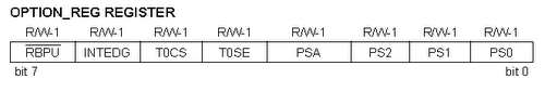
Initializing the OPTION_REG register
The following is an example how we can initialize the OPTION_REG:
- PSA=0; // Prescaler is assigned to the Timer0 module
- PS0=1; // Prescaler rate bits
- PS1=1; // are set to “111”
- PS2=1; // which means divide by 256
- TOSE=0; // rising edge
- TOCS=0; // Internal instruction cycle clock
Block diagram of the PIC Timer0 / WDT prescaler
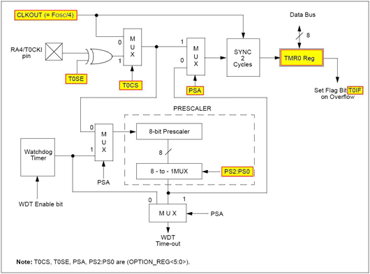
PIC TIMER0 block diagram
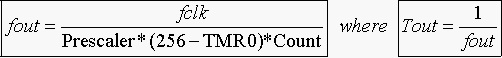
Calculating Count, Fout, and TMR0 values
If using INTERNAL crystal as clock, the division is performed as follow:
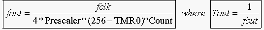
PIC TIMER0 formula for internal clock
Fout– The output frequency after the division.
Tout – The Cycle Time after the division.
4 - The division of the original clock (4 MHz) by 4, when using internal crystal as clock (and not external oscillator).
Count - A numeric value to be placed to obtain the desired output frequency - Fout.
(256 - TMR0) - The number of times in the timer will count based on the register TMR0.
An example of INTERNAL crystal as clock
Suppose we want to create a delay of 0.5 second in the our program using Timer0. What is the value of Count?
Calculation:
First, let’s assume that the frequency division by the Prescaler will be 1:256. Second, let’s set TMR0=0. Thus:
First, let’s assume that the frequency division by the Prescaler will be 1:256. Second, let’s set TMR0=0. Thus:
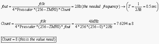
Formula to calculate Cout using Timer0
If using EXTERNAL clock source (oscillator), the division is performed as follow:
PIC TIMER0 formula for external clock
In this case there is no division by 4 of the original clock. We use the external frequency as it is.
An example of EXTERNAL clock source (oscillator):
What is the output frequency - Fout, when the external oscillator is 100kHz and Count=8?Calculation:
First, let’s assume that the frequency division by the Prescaler will be 1:256. Second, let’s set TMR0=0. Thus:
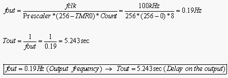
Formula to calculate Fout for Timer0
Delay of 1 sec using Timer0
The following simple program creates a delay of 1 sec using Timer0: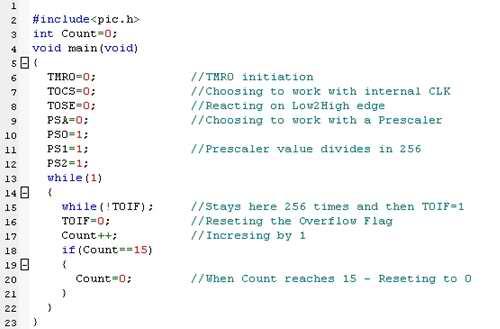
1 sec delay using Timer0
PIC Timer1 tutorial
The Timer1 module, timer/counter, has the following features:
- 16-bit timer/counter consisting of two 8-bit registers (TMR1H and TMR1L)
- readable and writable
- 8-bit software programmable prescaler
- Internal (4 Mhz) or external clock select
- Interrupt on overflow from FFFFh to 0000h
et’s explain the features of PIC Timer1 we have listed above:
Timer1 has a register called TMR1 register, which is 16 bits of size.
Actually, the TMR1 consists of two 8-bits registers:
Actually, the TMR1 consists of two 8-bits registers:
- TMR1H
- TMR1L
TMR1IF – TMR1 overflow Interrupt Flag bit.
This flag marks the end of ONE cycle count. The flag need to be reset in the software if you want to do another cycle count. We can read the value of the register TMR1 and write into. We can reset its value at any given moment (write) or we can check if there is a certain numeric value that we need (read).
This flag marks the end of ONE cycle count. The flag need to be reset in the software if you want to do another cycle count. We can read the value of the register TMR1 and write into. We can reset its value at any given moment (write) or we can check if there is a certain numeric value that we need (read).
Prescaler – Frequency divider.
We can use Prescaler for further division of the system clock. The size of the register is 2-bit only, so you can make four different division. The options are:
- 1:1
- 1:2
- 1:4
- 1:8
The structure of the T1CON register
We perform all the necessary settings with T1CON register. As we can see, the size of the register is 8 bits. Let’s explore the relevant bits: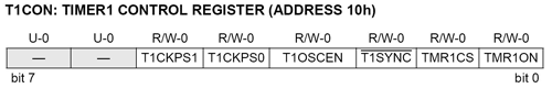
Initializing the T1CON register
The following is an example how we can initialize the T1CON register:- TMR1ON=1; // the timer is enable
- TMR1CS=0; // internal clock source
- T1CKPS0=0; // Prescaler value set to “00”
- T1CKPS1=0; // which means 1:1 (no division)
T1CON=0b00000001;
CLICK here for more information about PIC TIMER 1 Module
Block diagram of the PIC Timer1
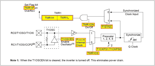
PIC TIMER1 block diagram
Calculating Count, Fout, and Timer1 values
If using INTERNAL crystal as clock, the division is performed as follow:
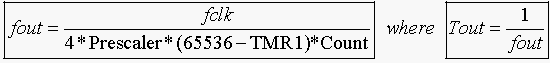
PIC TIMER1 formula for internal clock
Fout– The output frequency after the division.
Tout – The Cycle Time after the division.
4 - The division of the original clock (4 MHz) by 4, when using internal crystal as clock (and not external oscillator).
Count - A numeric value to be placed to obtain the desired output frequency - Fout.
(256 - TMR1) - The number of times in the timer will count based on the register TMR0.
If using EXTERNAL clock source (oscillator), the division is performed as follow:
PIC TIMER1 formula for external clock
Simple example and calculation of how to use TIMER1:
Suppose we want to create a delay of 2 second in the our program using Timer1. What is the value of Count?
Calculation:
First, let’s assume that the frequency division by the Prescaler will be 1:1. Second, let’s set TMR1=0, which means the TMR1 will count 65,536 times. Thus:
First, let’s assume that the frequency division by the Prescaler will be 1:1. Second, let’s set TMR1=0, which means the TMR1 will count 65,536 times. Thus:
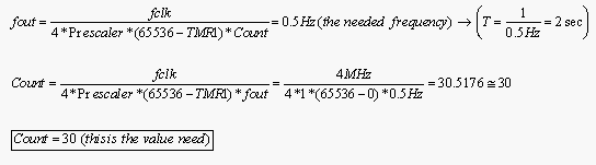
Formula to calculate Cout for Timer1
Delay of 1 sec using Timer1
The following simple program creates a delay of 1 sec using TIMER1:
#include<pic.h>

int Count = 0;
void main (void)
{
T1CON = 0b00000001;
while (1)
{
while (! TMR1IF);
TMR1IF = 0;
Count ++;
if (Count == 15)
{
Count = 0;
}
}
}
1 sec delay using Timer1
Timer2
The Timer2 module has the following features:
• two 8-bit registers (TMR2 and PR2)
• readable and writable
• prescaler and a postscaler
• connected only to an internal clock - 4 MHz crystal
• Interrupt on overflow
• two 8-bit registers (TMR2 and PR2)
• readable and writable
• prescaler and a postscaler
• connected only to an internal clock - 4 MHz crystal
• Interrupt on overflow
Let’s explain the features we have listed above:
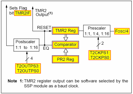
• Timer2 has 2 count registers: TMR2 and PR2. The size of each registers is 8-bit in which we can write numbers from 0 to 255. The TMR2 register is readable and writable and is cleared on any device Reset. PR2 is a readable and writable register and initialized to FFh upon Reset.
Register TMR2 is used to store the “initial” count value (the value from which it begins to count). Register PR2 is used to store the “ending” count value (the maximum value we need/want to reach). ie: using Timer2 we can determine the started count value, the final count value, and the count will be between these two values. The Timer2 increments from 00h until it matches PR2 and then resets to 00h on the next increment cycle.
Register TMR2 is used to store the “initial” count value (the value from which it begins to count). Register PR2 is used to store the “ending” count value (the maximum value we need/want to reach). ie: using Timer2 we can determine the started count value, the final count value, and the count will be between these two values. The Timer2 increments from 00h until it matches PR2 and then resets to 00h on the next increment cycle.
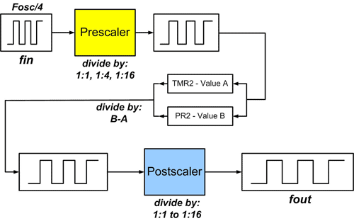
• Prescaler and Postscaler - Timer2 is an 8-bit timer with a prescaler and a postscaler. Each allows to make additional division of the frequency clock source.
Prescaler divides the frequency clock source BEFORE the counting take place at the register TMR2, thus the counting inside the TMR2 register is performed based on the divided frequency clock source by the Prescaler
The match output of TMR2 goes through a 4-bit postscaler (which gives a 1:1 to 1:16 scaling inclusive) to generate a TMR2 interrupt (latched in flag bit, TMR2IF (PIR1<1>)).
Postscaler divides the frequency that comes out of the Comparator again for the last time.
TIMER2 Prescaler and Postscaler
• TMR2IF - TMR2 to PR2 Match Interrupt Flag bit.
• Comparator – Compares the value of the register TMR2 and the maximum value of the register PR2.
• TMR2 – The register in which the “initial” count value is written.
• PR2 – The register in which the final or the maximum count value is written.
We perform all the necessary settings with T2CON Register The structure of the T2CON register:
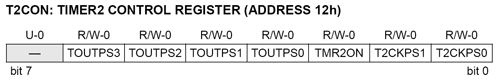
As we can see, the size of the register is 8 bits. Let’s explore the relevant bits:
T2CKPS1:T2CKPS0: Timer2 Clock Prescale Select bits
The input clock (FOSC/4) has a prescale option of 1:1, 1:4 or 1:16, selected by control bits T2CKPS1:T2CKPS0 (T2CON<1:0>).
The input clock (FOSC/4) has a prescale option of 1:1, 1:4 or 1:16, selected by control bits T2CKPS1:T2CKPS0 (T2CON<1:0>).
00 = Prescaler is 1
01 = Prescaler is 4
1x = Prescaler is 16
01 = Prescaler is 4
1x = Prescaler is 16
TMR2ON: Timer2 On bit
Timer2 can be shut-off by clearing control bit, TMR2ON (T2CON<2>), to minimize power consumption.
Timer2 can be shut-off by clearing control bit, TMR2ON (T2CON<2>), to minimize power consumption.
1 = Timer2 is on
0 = Timer2 is off
0 = Timer2 is off
TOUTPS3:TOUTPS0: Timer2 Output Postscale Select bits
The match output of TMR2 goes through a 4-bit postscaler (which gives a 1:1 to 1:16 scaling inclusive selected by control bits TOUTPS3:TOUTPS0 (T2CON<6:3>).
The match output of TMR2 goes through a 4-bit postscaler (which gives a 1:1 to 1:16 scaling inclusive selected by control bits TOUTPS3:TOUTPS0 (T2CON<6:3>).
0000 = 1:1 postscale
0001 = 1:2 postscale
0010 = 1:3 postscale
•
•
•
1111 = 1:16 postscale
0001 = 1:2 postscale
0010 = 1:3 postscale
•
•
•
1111 = 1:16 postscale
The following is an example how we can initialize the T2CON register:
1. TMR2ON=1; // the timer is enable
2. T2CKPS0=0; // Prescaler – 1:1
3. T2CKPS1=0;
2. T2CKPS0=0; // Prescaler – 1:1
3. T2CKPS1=0;
4. TOUTPS0=1; // Postscaler – 1:16
5. TOUTPS0=1;
6. TOUTPS0=1;
7. TOUTPS0=1;
5. TOUTPS0=1;
6. TOUTPS0=1;
7. TOUTPS0=1;
Or you can set all the T2CON register at once as follows:
T2CON=0b01111100;
T2CON=0b01111100;
TIMER2 BLOCK DIAGRAM
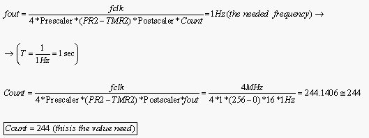
How to calculate the required values of the TIMER2:

Fout – The output frequency after the division.
Tout – The Cycle Time after the division.
4 - The division of the original clock (4 MHz) by 4, when using internal crystal as clock (and not external oscillator).
Count - A numeric value to be placed to obtain the desired output frequency - fout.
(PR2 – TMR2) - The number of times the counter will count.
Simple example and calculation of how to use TIMER2:
Suppose we want to create a delay of 1 second in the our program using Timer2. What is the value of Count?
Calculation:
First, let’s assume that the frequency division by the Prescaler will be 1:1 and Postscaler will be 1:16. Second, let’s set TMR1=0 and PR2=255. Thus:
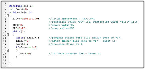
The following simple C language program creates a delay of 1 sec using TIMER2: